XLRN 801.CR - Introduction to Microchip Fabrication
35433569
Loading...
Course Description
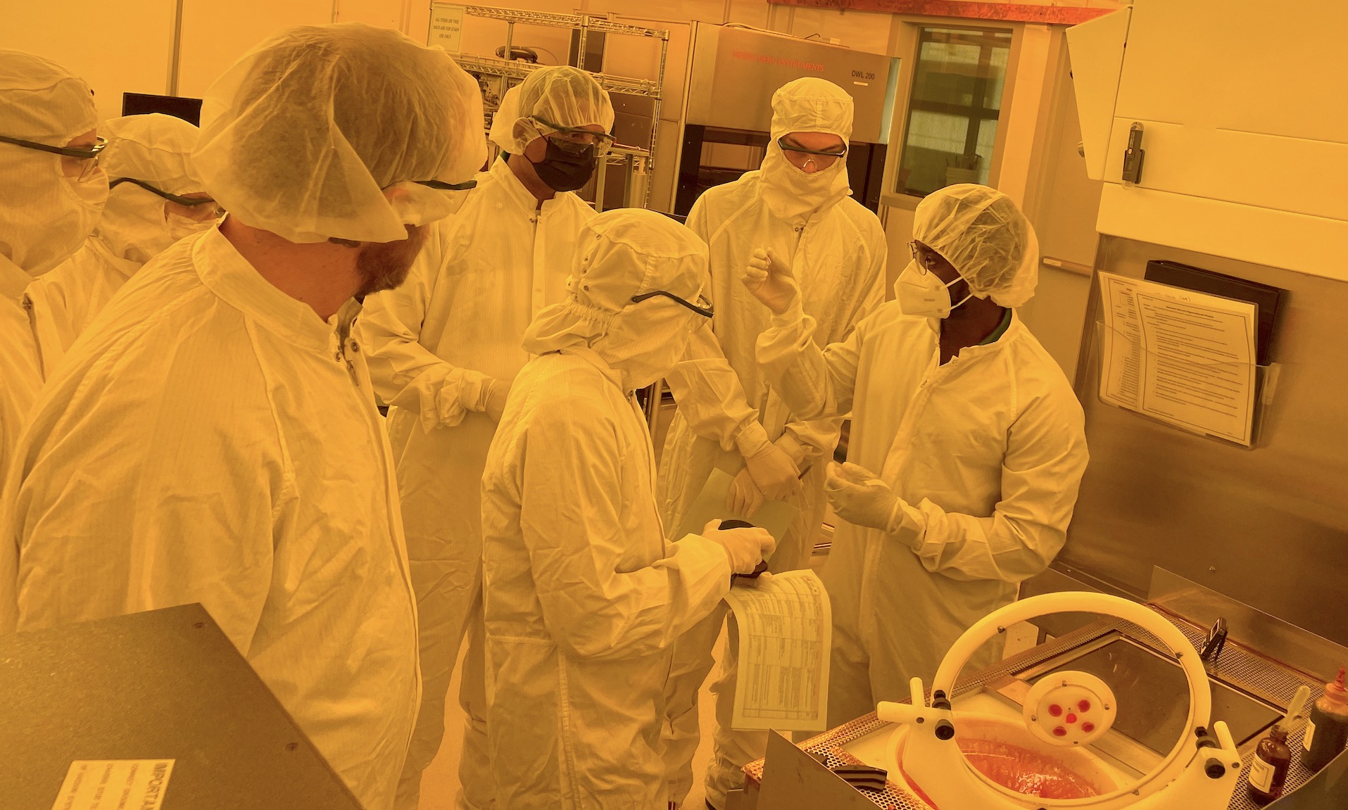
Our hand-on trainings are designed for professionals or new entrants wanting to upskill their this semiconductor expertise in a cleanroom environment. Students will learn the practical protocols and procedures you need for safe and successful participation in a cleanroom.
This course serves as first step towards the Cleanroom Technician training.
Individual enrollments: self-enroll on this page
Group enrollments: please contact us at help@professional.ucsb.edu
Course Outline
Once enrolled, please complete:
| Topic | Duration (hours) |
| DAY 1 | |
| Industry Introduction (what/who/jobs) | 1 |
| Lab Safety | 1 |
| Cleanroom & Gowning & PPE | 0.5 |
| Semiconductor Basics: Substrates, Photolithography, Etch, Deposition | 1.5 |
| LUNCH | |
| CLEANROOM: Gowning, Art Wafer Resist Spin, Filmetrics, Dektak | 4 |
| DAY 2 | |
| Electrostatic discharge (ESD) / Statistical Process Control / Quality Systems | 1 |
| Metrology / Gage R&R | 1 |
| Wafer Handling / Passdown/Automated Travelers / Recording+Reporting Observations | 1 |
| LUNCH | |
| CLEANROOM: Etch Art Wafers, Microscope, Handling | 4 |
| Summary | 0.5 |
| Evaluation | 0.5 |
| Total | 16 |
Learner Outcomes
Upon successful completion of this course, students will have been introduced to:- What a career in the semiconductor industry entails
- Further study in the Cleanroom Technician course
- Semiconductor processes: Photolithography, Deposition, Etch and Metrology
- Gowning Protocol
- Wafer Handling; Use of Microscope; ESD; Metrology
- Statistical Process Control
Loading...